A glowing blue diagram of a CPU architecture shows three registers R1, R2, R3, an ALU, a common data bus, and a clock signal, detailing operations across three cycles.
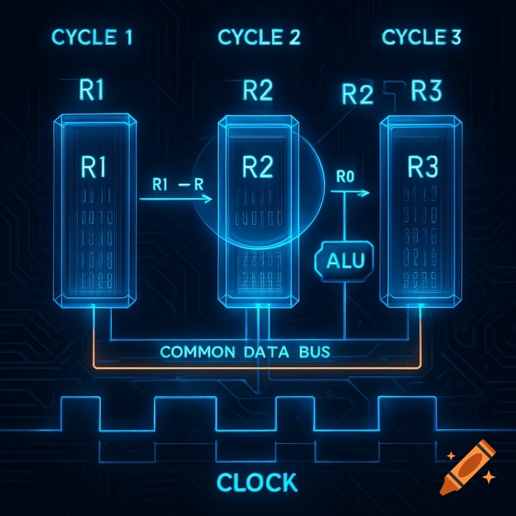
The following question represents a simplified CPU with three registers: R1, R2, and R3, and a common bus controlled by a clock signal. 1. On paper, draw a register transfer diagram showing R1, R2, R3, the bus, and the control signals (Load, Enable, Clock). 2. Show how the following operation would be executed across three clock cycles: • Cycle 1: Move the contents of R1 to R2 • Cycle 2: Add 1 to R2 (assume there is a simple ALU connected to the bus) • Cycle 3: Store the result into R3 3. Label on your diagram: • What each register is doing in each cycle • When the clock edge occurs • When data is on the bus or being latched 4.Additional questions: • What ensures that R3 doesn’t receive the data too early or too late? • Why do all registers share the same clock? See more