A hand-drawn doodle of a CPWG PCB cross-section, showing signal and ground traces with dimensions W, S, H, and associated characteristic impedance formulas handwritten next to it.
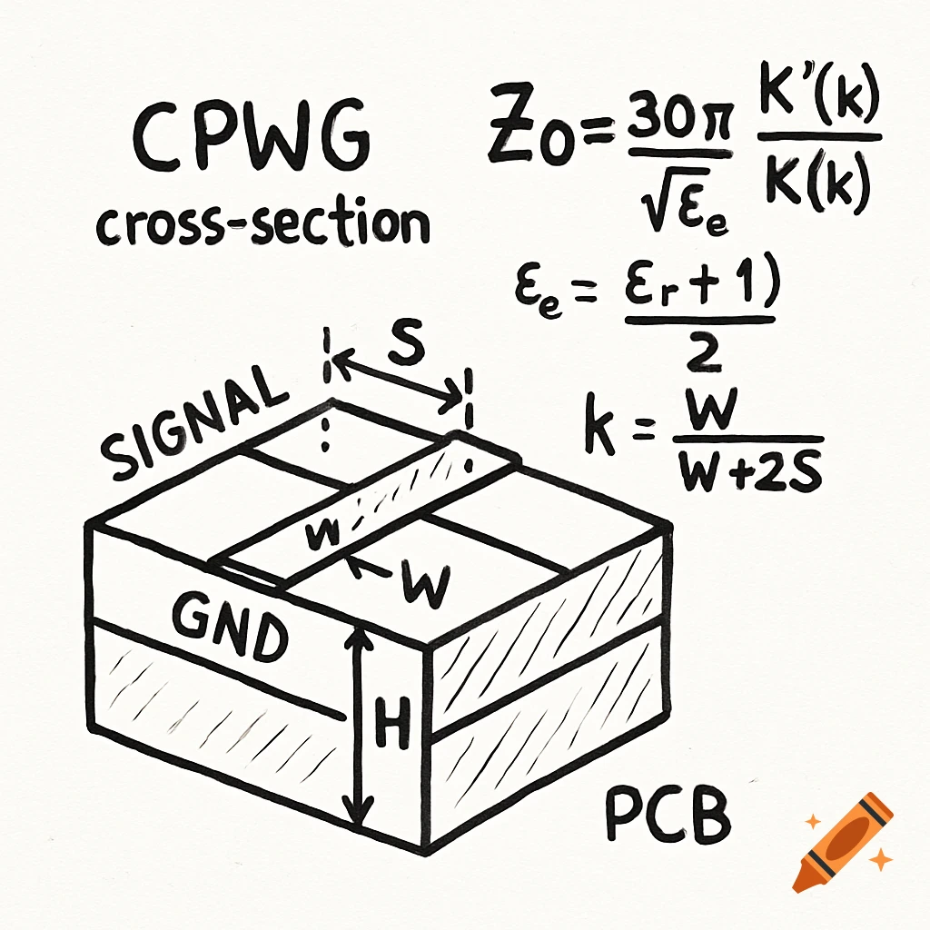
A playful, hand-drawn doodle style illustration of a Coplanar Waveguide (CPWG) PCB cross-section from a slightly elevated, angled perspective. Show the central signal trace (W) flanked by two ground planes (GND) with gaps (S) in between them, all on top of a dielectric substrate (H). Include dashed lines and arrows indicating the dimensions W, S, and H. Next to or integrated into this doodle, handwritten in a clear, easy-to-read doodle font, is the characteristic impedance formula for CPWG: Z_0 = (30 * pi / sqrt(epsilon_e)) * (K'(k) / K(k)). Also, show the definitions for epsilon_e = (epsilon_r + 1)/2 and k = W / (W + 2S). The overall aesthetic should be like a sketch on a whiteboard or notebook, friendly and illustrative, suitable for a presentation. See more