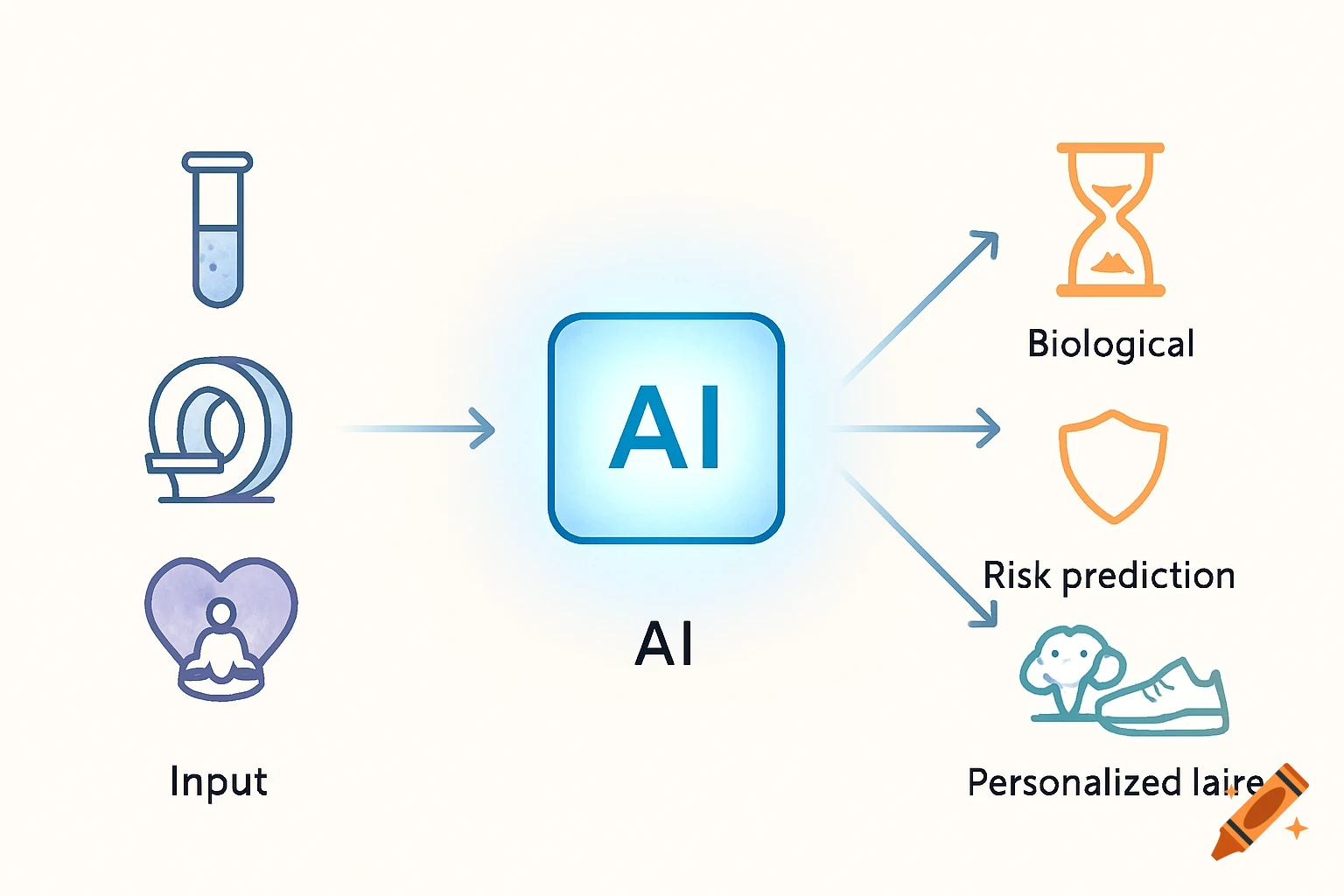
A scientific illustration shows an AI system assisting in semiconductor device design, leading to enhanced process development and superior device efficiency. It depicts AI icon, graphs, FinFET and GAAFET structures, fabrication steps, and a silicon wafer.
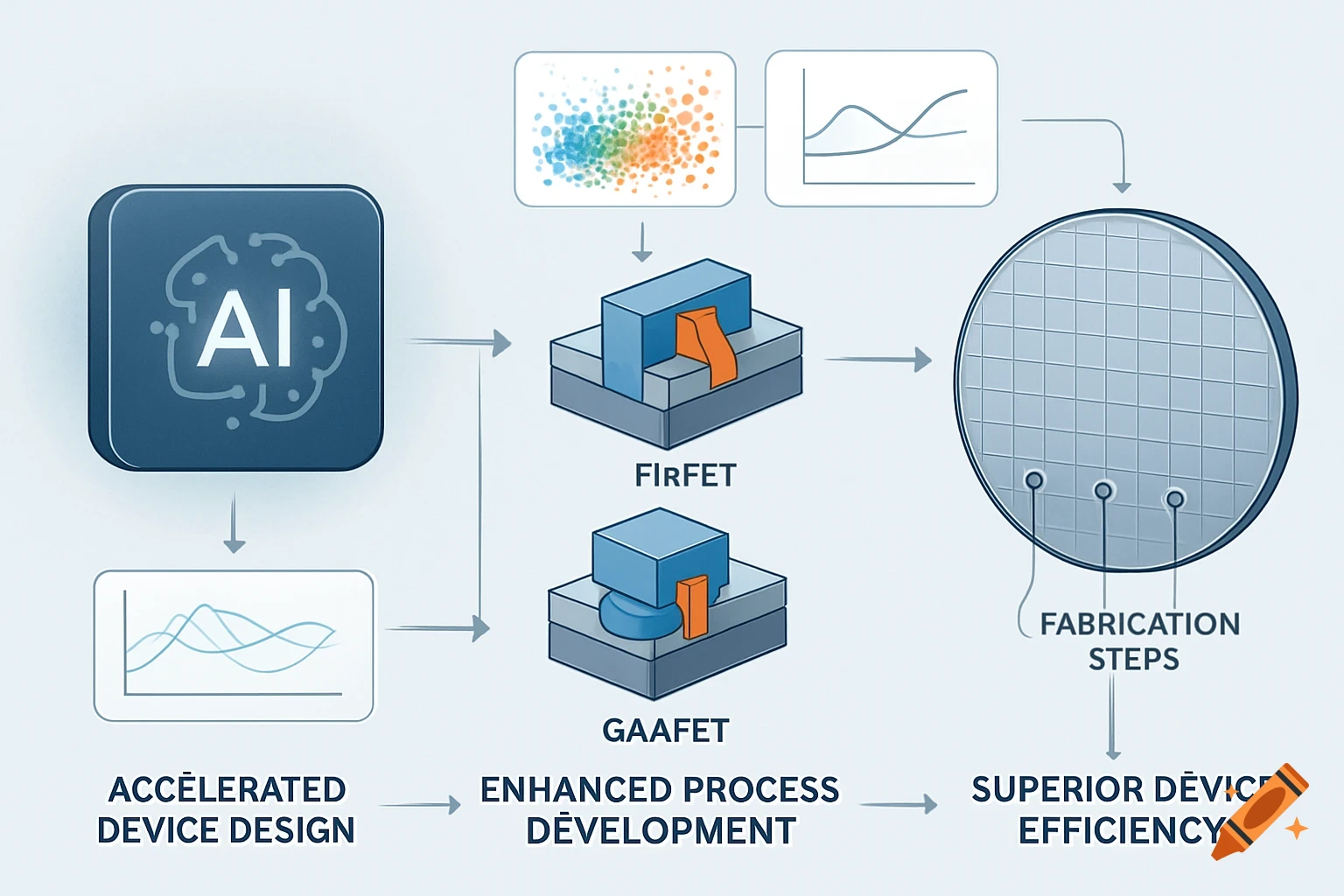
A clear, professional scientific illustration showing an AI system helping design and improve semiconductor electron devices. The image should show a simple workflow: AI models analyze data → predict optimal process parameters → guide experiments → evaluate device performance and yield. Include nanoscale transistor structures (FinFET or GAAFET or CFET), clean graphs or simulation outputs, and a wafer or fabrication step to represent manufacturing. The overall concept should communicate that AI accelerates device design, speeds up process development, and improves performance and efficiency. Use a clean, modern, high-tech style suitable for a research presentation. Avoid futuristic sci-fi elements and avoid robotic arms. Keep the composition simple, scientific, and realistic. See more